
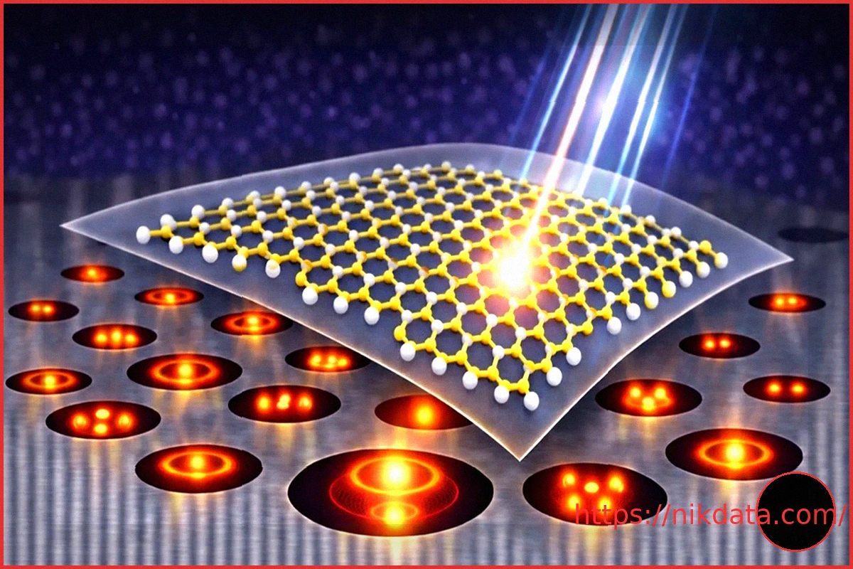
Scientists have discovered an ingenious method to enhance the performance of ultra-thin semiconductors, not by altering their intrinsic material properties, but by cleverly reshaping the immediate environment beneath them. This groundbreaking technique involves precisely placing a single-atom-thick layer of tungsten disulfide over tiny, engineered air cavities carved into a crystal lattice. These meticulously crafted hollow structures, known as “Mie voids,” function as highly efficient miniature light traps.
By concentrating light exactly where the atomic-scale semiconductor material is situated, these innovative traps significantly amplify its optical effects. The results are striking: a dramatic boost in brightness, exhibiting up to 20 times stronger light emission, and an astonishing 25 times stronger nonlinear optical signals. This novel design effectively overcomes a significant limitation inherent in atomically thin devices, paving the way for more powerful and efficient next-generation electronics and photonics.